PDMS (polydimethylsiloxane) stamps are key tools in micro- and nanofabrication and are usually prepared by photolithography. In Microcontact Printing, PDMS stamps act as soft templates with the ability to efficiently transfer tiny patterns.
Its flexibility and ease of preparation have led to its widespread use in the preparation of biochips, biosensors and microelectronic devices. In the development of PDMS stamps, it has gone through several stages and also faced some challenges.
At the current stage, researchers are trying to solve these challenges and seek wider application areas. In this paper, the development process of PDMS stamp, challenges at the current stage, future directions, and application scenarios will be explained.
1 Development Process of PDMS Stamps
1.1 Early Stages
PDMS, as a flexible material, was initially used for fabricating flexible templates in the early stages. However, due to limitations in fabrication techniques, the transfer of patterns at the micro and nanoscale was not ideal.
1.2 Introduction of Photolithography
With the continuous advancement of photolithography techniques, the fabrication process of micro stamps improved. The introduction of photolithography allowed precise patterning on the surface of PDMS, enhancing the stamp's resolution and transfer efficiency.
1.3 Optimization of Surface Treatment
To further enhance the performance of PDMS stamps, researchers implemented various surface treatments, such as coatings and functional modifications on PDMS surfaces. These optimizations aimed to improve adhesion to different materials, thus expanding the application range.
2 Current Challenges
2.1 Precision and Consistency in Fabrication
While the application of photolithography has improved the precision of micro stamps, maintaining consistency in the fabrication process remains a challenge in large-scale production. Ensuring identical performance for each stamp is a current issue.
2.2 Durability and Stability
PDMS material may undergo aging after prolonged use, affecting the stability and durability of stamps. Particularly in biomedical applications, higher demands are placed on material biocompatibility and long-term stability.
2.3 Fabrication Costs
Although PDMS fabrication is relatively straightforward, cost remains a consideration in large-scale production. Reducing the cost of PDMS stamp fabrication to enhance competitiveness is a current concern.
3 Future Directions
3.1 Introduction of New Materials
Researchers are exploring novel elastic materials to replace or improve PDMS, aiming to enhance stamp performance and stability. Examples include new polymers similar to PDMS or materials with improved biocompatibility.
3.2 Innovative Fabrication Techniques
As nanotechnology continues to advance, new fabrication techniques emerge. The introduction of techniques such as atomic layer deposition and nanoimprint lithography holds the potential to improve the precision and efficiency of PDMS stamp fabrication.
3.3 Design of Multifunctional Stamps
Future directions also include designing multifunctional PDMS stamps with a broader range of applications. For instance, integrating biosensor technology could enable PDMS stamps to not only transfer patterns but also detect target substances during the transfer process.
4 Applications of PDMS Stamps
4.1 Preparation of Biochips
PDMS stamps find widespread application in the preparation of biochips, efficiently transferring small biological patterns for applications in cell culture and analysis.
4.2 Biosensors
Micro stamps can be used to fabricate microstructures for biosensors, enabling the detection of biomolecules and cells with promising applications.
4.3 Microelectronic Devices
PDMS stamps play a crucial role in the fabrication of microelectronic devices, including the preparation of flexible electronic devices and microelectrode arrays.
Overall, PDMS stamps, as critical tools in micro and nanofabrication, hold significant potential in biomedical and microelectronic fields. With continuous technological development and innovation, PDMS stamps are expected to better meet the diverse needs of various fields, providing robust support for the advancement of micro-nanofabrication technologies.
5 Microcontact Printing
Microcontact Printing (μCP) is a nanomanufacturing technique primarily used to transfer materials onto the surface of substrates at the micro and nanoscale. It is a highly precise printing technology widely applied in biomedical, nanoelectronics, and sensor manufacturing fields. The overview of Microcontact Printing includes:
Basic Principles: Microcontact Printing operates on the fundamental principle of using elastic templates, such as silicon rubber, with patterns or molecules on their surfaces. By bringing the template into contact with the substrate, the material is transferred from the template to the substrate, forming the desired pattern.
Material Selection: The key to Microcontact Printing lies in selecting appropriate materials. Typically, silicon rubber serves as the elastic template, while substrates can be various materials, including metals, glass, and polymers. The imprinted material may include organic molecules, nanoparticles, and biological molecules.
Template Fabrication: The fabrication of templates is a critical step in Microcontact Printing. Common methods include photolithography, electron beam exposure, and other micro-nanofabrication techniques to create the desired patterns on the template surface.
Transfer Process: During contact between the elastic template and the substrate, the material is transferred to the substrate surface through intermolecular forces. This transfer process usually occurs at room temperature without requiring high temperatures or pressure.
Application Areas: Microcontact Printing is commonly used in biomedical applications for the fabrication of biochips, biosensors, and more. In nanoelectronics, it can be employed for the preparation of nanocircuits and sensors. Additionally, Microcontact Printing finds applications in surface treatments and nanooptical devices.
Advantages: The advantages of Microcontact Printing include its simplicity, cost-effectiveness, high resolution, and precision. Moreover, it allows for patternization on different types of surfaces.
It's important to note that while Microcontact Printing has widespread applications, it may need to be combined with other manufacturing technologies for specific requirements, such as ultra-high resolution and large-area coverage.
DXFLUIDICS
Dxfluidics showcases outstanding capabilities in PDMS stamp and micro well arrays processing. Through advanced micro-nanofabrication techniques and the support of a professional team, the company can precisely manufacture high-resolution micro well arrays for applications like microcontact printing. With rich experience in photolithography techniques and optimized surface treatment technologies, Dxfluidics ensures excellent performance of micro well arrays in transferring small patterns. Whether it's the preparation of biochips, biosensors, or microelectronic devices, Dxfluidics is committed to providing customized solutions to meet high customer requirements. Through continuous innovation and technical excellence, Dxfluidics has established a solid reputation in the field of PDMS stamp processing.

| Product Code | Dimensions-Size (mm) | Micro needle size | 模具 Material | 印章 Material | Price (¥) | ||
| Height (mm) | 底部Diameter (mm) | Space (mm) | |||||
| 200001 | heart-shaped-15*12.8 | 1 | 0.5 | 1 | HTL | PDMS | 200 |
| 200002 | square-12*12 | 1 | 0.5 | 1 | HTL | PDMS | 200 |
| 200003 | square-11*11 | 0.6 | 0.25 | 0.5 | HTL | PDMS | 200 |

| 产品 编号 | Dimensions (mm) | Microcolumn dimensions | 模具 Material | norm | Price (¥) | ||
| Height (um) | Diameter (mm) | Space (mm) | |||||
| 200004 | 16*16 | 200 | 0.2,0.4,0.6,0.8 | 1 | SU8 | PDMS微坑 | 200 |
| 200005 | 16*16 | 200 | 0.2,0.4,0.6,0.8 | 3 | SU8 | PDMS微坑 | 200 |
| 200006 | 16*16 | 100 | 0.1,0.2,0.3,0.4 | 1 | SU8 | PDMS微坑 | 200 |
| 200007 | 16*16 | 5 | 0.005(5um) | 0.005 | SU8 | PDMS微坑 | 200 |
| 200008 | 16*16 | 10 | 0.005(5um) | 0.005 | Si | PDMS微坑 | 200 |

| 产品编号 | Dimensions (mm) | Microcolumn dimensions | 模具Material | norm | Price (¥) | ||
| Height (um) | Diameter/Width (mm) | Space (mm) | |||||
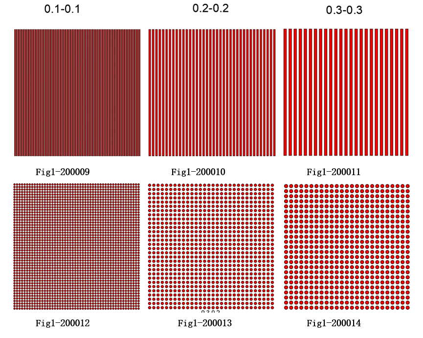
| 200009 | 16*16 | 100 | 0.1 | 0.1 | SU8 | PDMS微柱 | 200 |
| 200010 | 16*16 | 100 | 0.2 | 0.2 | SU8 | PDMS微柱 | 200 |
| 200011 | 16*16 | 100 | 0.3 | 0.3 | SU8 | PDMS微柱 | 200 |
| 200012 | 16*16 | 100 | D0.2 | 0.1 | SU8 | PDMS微柱 | 200 |
| 200013 | 16*16 | 100 | D0.3 | 0.2 | SU8 | PDMS微柱 | 200 |
| 200014 | 16*16 | 100 | D0.4 | 0.2 | SU8 | PDMS微柱 | 200 |

| Product Code | Dimensions (mm) | Shape | norm | Microcolumn dimensions | 价格(¥)/片 | ||
| Height | 直径/宽度 | Space | |||||
| (um) | (um) | (um) | |||||
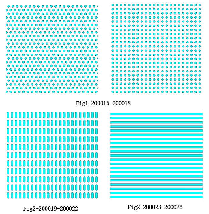
| 200015 | 10*10 | circle | PDMS微柱/坑 | 10 | 5 | 10 | 200 |
| 200016 | 10*10 | circle | PDMS微柱/坑 | 10 | 10 | 20 | 200 |
| 200017 | 10*10 | circle | PDMS微柱/坑 | 10 | 20 | 40 | 200 |
| 200018 | 10*10 | circle | PDMS微柱/坑 | 10 | 50 | 100 | 200 |
| 200019 | 10*10 | 环 | PDMS微柱/坑 | 10 | 5 | 15 | 200 |
| 200020 | 10*10 | 环 | PDMS微柱/坑 | 10 | 10 | 30 | 200 |
| 200021 | 10*10 | 环 | PDMS微柱/坑 | 10 | 20 | 60 | 200 |
| 200022 | 10*10 | 环 | PDMS微柱/坑 | 10 | 50 | 150 | 200 |
| 200023 | 10*10 | 长条 | PDMS微柱/坑 | 10 | 5 | 15 | 200 |
| 200024 | 10*10 | 长条 | PDMS微柱/坑 | 10 | 10 | 30 | 200 |
| 200025 | 10*10 | 长条 | PDMS微柱/坑 | 10 | 20 | 60 | 200 |
| 200026 | 10*10 | 长条 | PDMS微柱/坑 | 10 | 50 | 150 | 200 |
© 2025. All Rights Reserved. 苏ICP备2022036544号-1


