Currently, most of the methods used by researchers to process 3D microfluidic chip microchannels are based on photolithography, but photolithography is mainly used to fabricate high-resolution 2D microchannels, and it is still immature to apply it to the preparation of 3D microfluidic channels.
In the following, the fabrication techniques of 3D microfluidic chips are summarized from microfabrication technology and 3D printing technology, mainly introducing microfilament plastic molding method, embedded sacrificial element method, stacking method, femtosecond laser method and light curing.
1. Microprocessing technologies
Micromachining is a high-precision fabrication technique used to create micron- and nanoscale structures for a wide range of applications in electronics, medicine, biotechnology and microfluidics. It is ideal for 3D microfluidic chip fabrication because of its high resolution and wide applicability.
In this paper, we will focus on several methods in microfabrication technology: microfilament plastic molding, embedded sacrificial element method, stacking, femtosecond laser method and paper-based method.
Microfiber Molding
Microfiber Molding creates microchannels in polymer films by using micron-sized fibers or wires as molds.
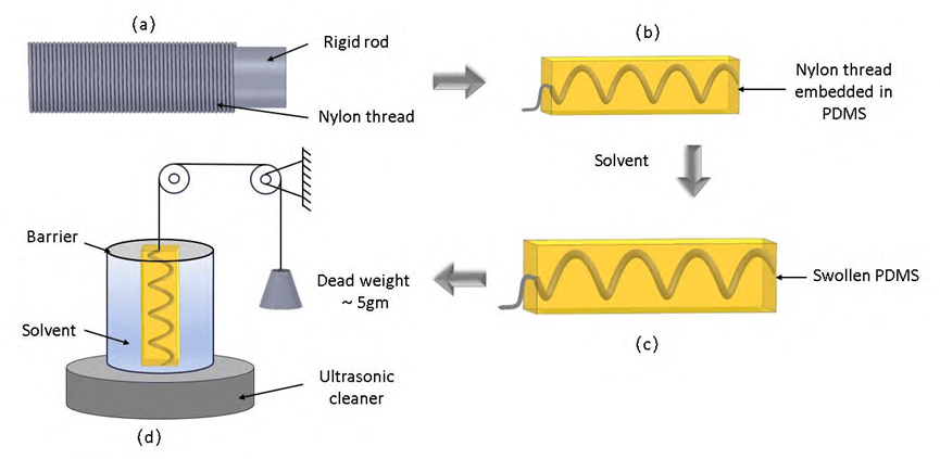
Start by selecting a suitable transparent substrate material such as polydimethylsiloxane (PDMS), polycarbonate (PC) or polymethylmethacrylate (PMMA).
Fibers or wires are arranged on the substrate according to the desired structure, and these fibers may be arranged singly or in multiples to form grids, lines, or other patterns. The substrate and the fiber template are then placed into a plastic molding apparatus so that the fibers are embedded in the substrate to form microchannels.
After the substrate has cured, the template is gently removed to leave the desired microchannel.
2) Embedded Sacrificial Element Method
Embedded Sacrificial Element Method (ESEM) is a low-cost microfluidic chip fabrication technique.
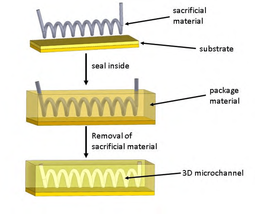
In this method, a sacrificial material is immobilized on the substrate to form a 3D structure, and subsequently an encapsulation material is cast onto the sacrificial material to construct a 3D microfluidic network.
After the encapsulation material is cured, the sacrificial structure is removed to obtain a microfluidic chip with 3D microchannels.
3) Stacking method
In microfluidic chip preparation, Stacking is a commonly used technique for building microfluidic chips with multilayer structures.

First, the hierarchical structure of the chip is designed to clarify the function and layout of each layer. Substrate materials are usually chosen from transparent polymers such as polycarbonate (PC), polymethylmethacrylate (PMMA) or PDMS.
Next, the desired microchannels are prepared on each substrate using micro-nanofabrication techniques such as photolithography, electron-beam exposure, or laser processing, and the structure can be either single-layer or multilayer, depending on the design requirements. Finally, the layers of substrates are stacked together to form a microfluidic chip with a multilayer structure.
4) Femtosecond laser method
Femtosecond Laser Method (FMLM) is an advanced technology for microfluidic chip fabrication that utilizes femtosecond laser processing of microchannels.
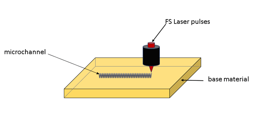
Femtosecond lasers are ultrashort pulsed lasers with pulse widths typically in the femtosecond range (1 fs = 10^-15 seconds), capable of generating very high power densities in very short periods of time.
When the laser is focused on the surface of the material, the resulting high light intensity triggers a non-thermal process that results in the direct removal of the material without transferring heat to the surrounding area.
Femtosecond laser technology has been widely used in the fabrication of hybrids, biomedicine, algae screening and 3D microfluidic channels.
5)Paper-based Method
Paper-based Method (PBM) is an innovative microfluidic chip fabrication technology based on the traditional paper folding principle.
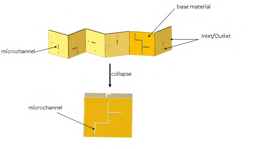
The method begins with the selection of a suitable substrate, which is commonly used as a soft, transparent and easy-to-process material such as PDMS.
Next, the geometry of the microchannel is designed and the substrate is cut into predefined shaped segments by laser cutting or CNC cutting.
The segments were then folded according to a folding scheme to form a 3D microfluidic structure.
The advantages of this technology are simplicity and low cost, eliminating the need for expensive equipment and complex steps compared to traditional micromachining techniques, making it suitable for rapid, low-cost manufacturing needs such as disposable biosensors and portable diagnostic devices.
2. 3D printing technology
1) SLA Technology
SLA technology utilizes photosensitive resins, which are special liquid materials capable of undergoing a photopolymerization reaction under ultraviolet (UV) irradiation to change from a liquid to a solid state.
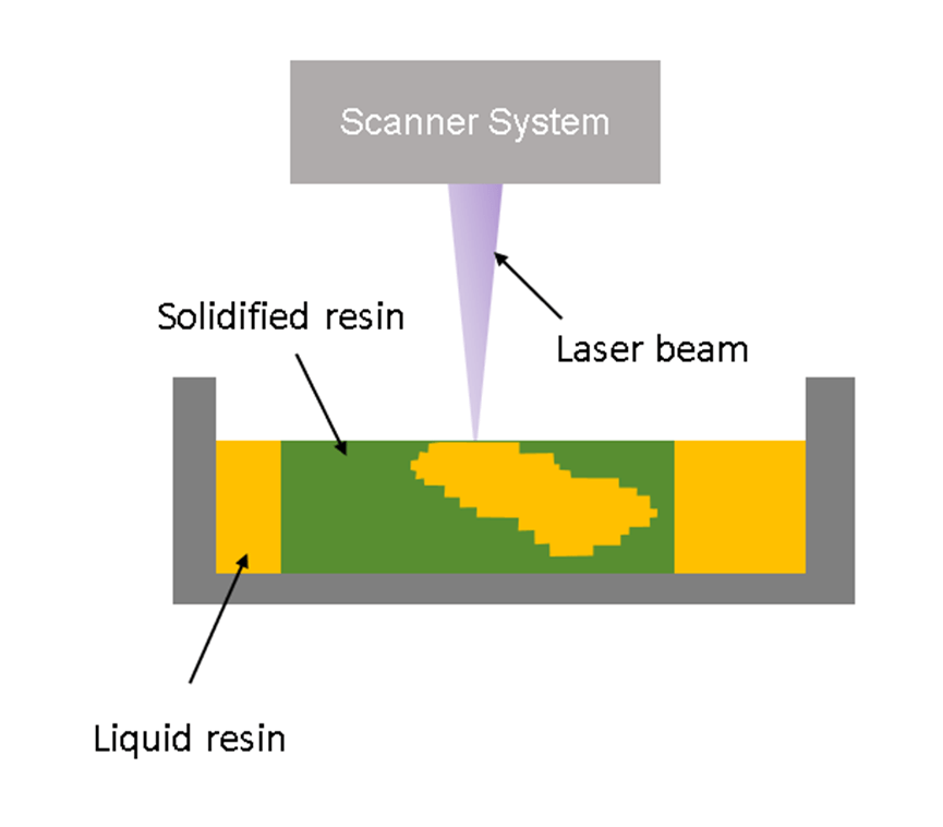
First, a thin layer of photosensitive resin is applied to the table; next, a UV laser beam is used to precisely scan and cure specific areas of the resin to form the shape of the layer. After completing a layer, the table is lowered to the next layer and a new liquid resin is applied again.
The laser beam is then scanned along the contours of the new cross-section, curing the new layer. This process is repeated until the entire structure is built.
2) Extrusion-based 3D printing technology
Extrusion-based fused deposition molding (FDM) processes are commonly used for the preparation of 3D microfluidics.FDM technology uses thermoplastic materials, typically acrylonitrile butadiene styrene (ABS) or polylactic acid (PLA), which are coiled in a thread-like form on a spool of filler.
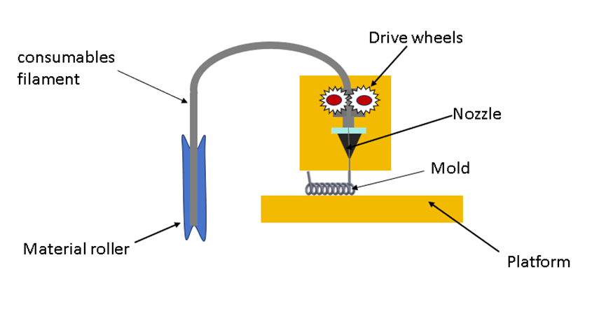
The filament is fed into a heated extruder head, which can be moved horizontally and vertically, and melted into a liquid state. The printer stacks the molten material layer by layer on the build platform based on the hierarchical information generated by slicing the 3D model.
After each layer solidifies, the printer moves to the next layer and repeats the process until the entire model is printed. Subsequent processing is similar to the sacrificial material in the sacrificial element method, resulting in the desired 3D microfluidic structure.
FDM technology has the advantages of low cost, high sensitivity and ease of operation, but its print surface quality is poorer than other high-precision technologies, and the support structures generated during printing need to be removed manually, increasing the complexity of subsequent processing.
3) Inkjet 3D Printing Technology
Inkjet 3D printing technology is a novel 3D printing method that differs from traditional layer stacking techniques such as FDM. Instead of using fused filaments or light-curing resins, inkjet 3D printing builds objects by spraying them with a liquid material, such as a suspension of polymers, ceramics, or metal particles.
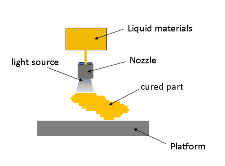
The inkjet head ejects liquid material in tiny droplets onto the build platform and cures the material in the droplets using UV or other light sources. The printing process proceeds layer by layer, with the inkjet head accurately ejecting the liquid material based on the designed 3D model, gradually stacking it to form the target structure.
After printing, curing or drying is required to ensure the stability and hardness of the object. In addition, the technology allows for the construction of channel graphics with different structures as needed.
Site Search
Recommendations
© 2025. All Rights Reserved. 苏ICP备2022036544号-1


