The PDMS Chip Processing Platform is designed to provide an efficient and comprehensive solution for the preparation of PDMS chips.
This platform integrates electronic scales, PDMS chip pouring devices, ovens, PDMS chip punching machines, PDMS chip cutting tools, PDMS chip aligners, as well as PDMS plasma bonding machines and other PDMS chip processing equipment.
With its professional design, the PDMS Pourer enables the PDMS material to be poured uniformly onto the mold, providing support for chip forming.
The oven provides stable temperature control to ensure adequate curing of the PDMS material.
The PDMS punch and cutter ensures precise hole and structure fabrication, providing greater machining accuracy.
The PDMS aligner, on the other hand, enables precise alignment of multilayer structures and enhances the ability to fabricate multilayer PDMS chips.
The plasma bonding machine realizes the strong bonding of PDMS.
The compact design of the processing platform makes it easy to be deployed in ordinary laboratories and helps customers to quickly realize chip preparation, providing convenient and powerful support for research and application of microfluidic technology.
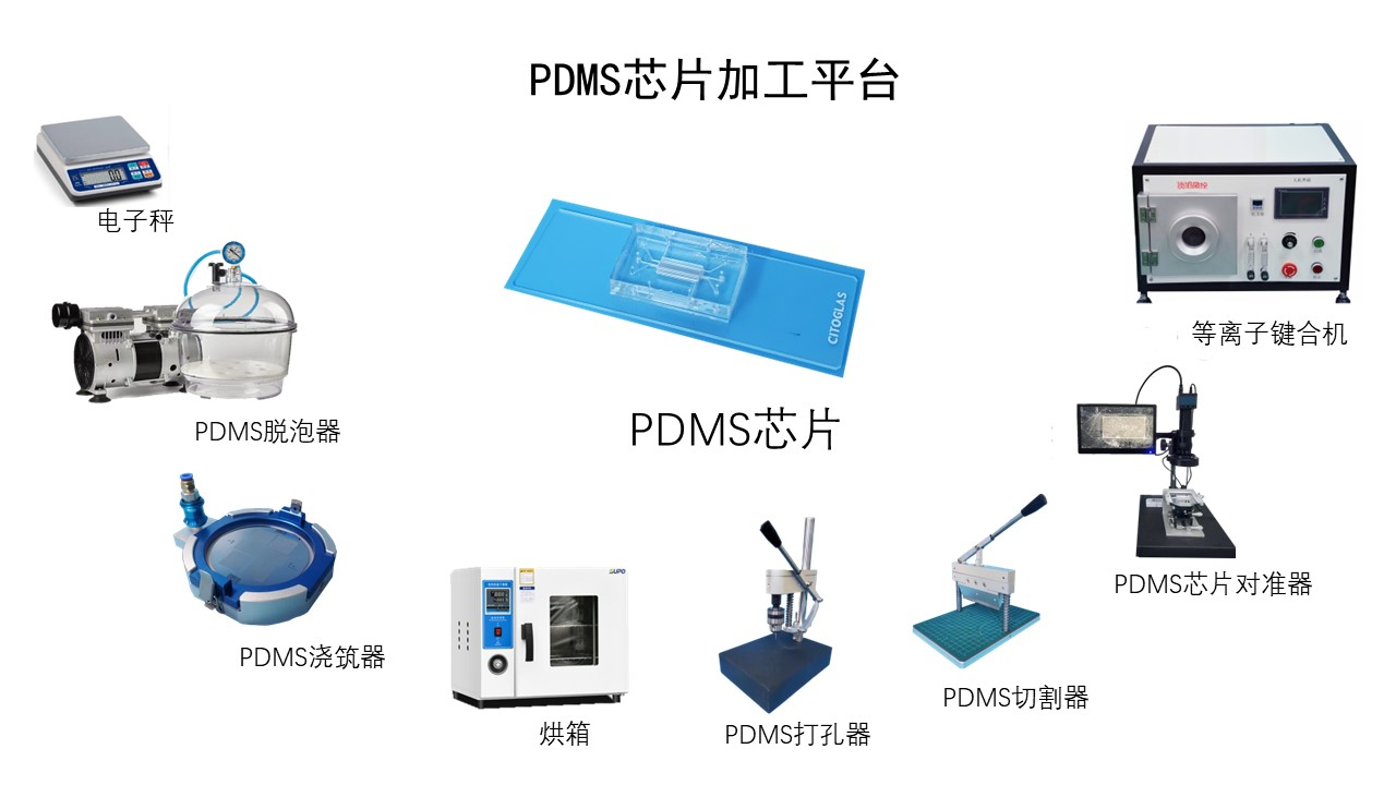
2 PDMS Chip Processing Equipment
2.1 Electronic Scale
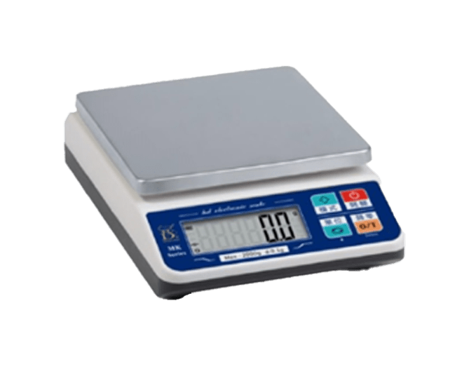
- > Range : 0.01~1000g
- > Accuracy: 0.01g
- > Square Tray Size: 16x18cm
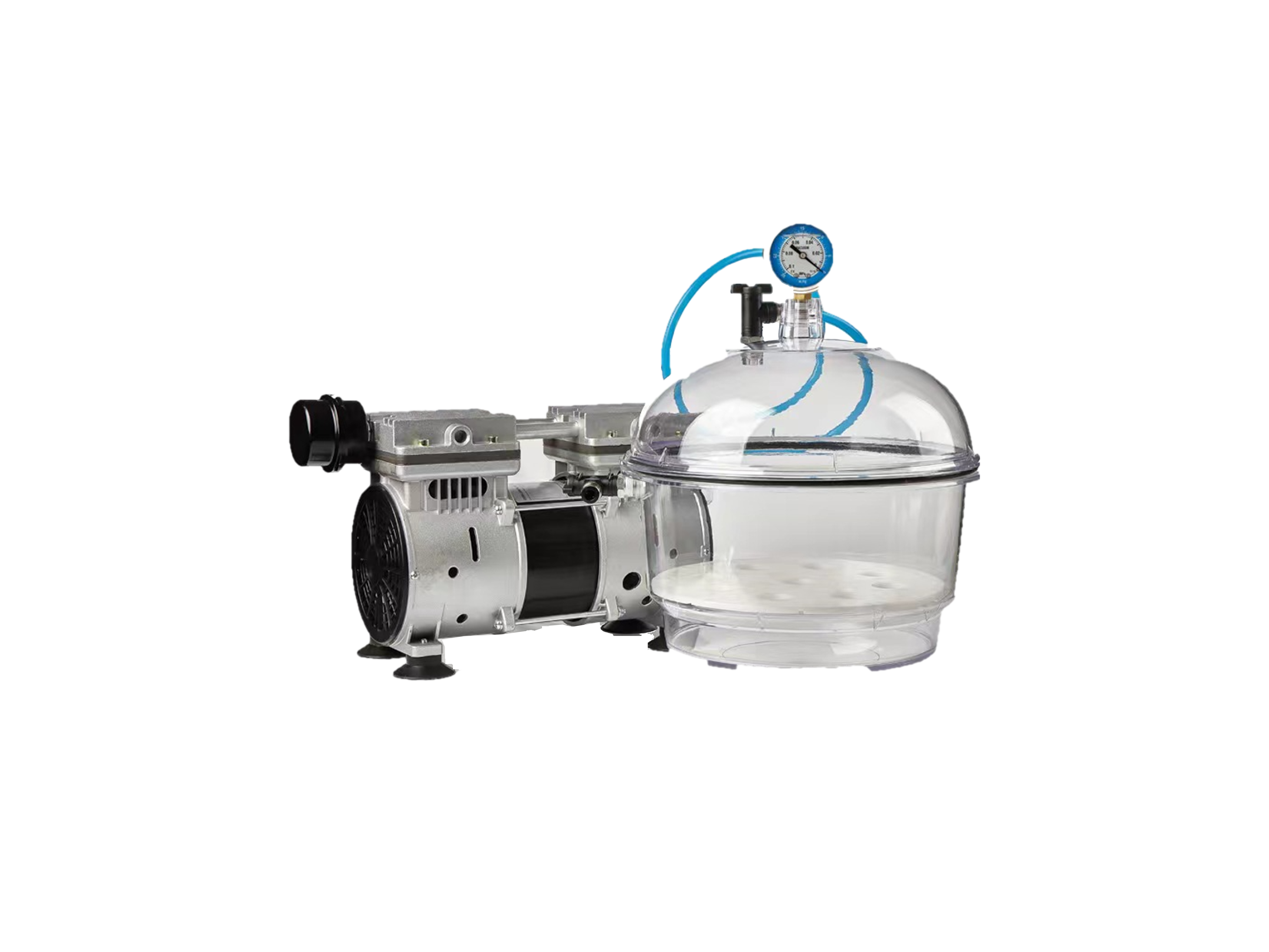
2.2 Debubbler

- Material: PC
- Baffle Diameter: 230mm
- High-quality silicone O-ring seal maintains high vacuum
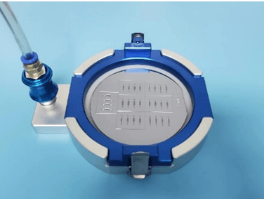
2.3 PDMS Casting Device
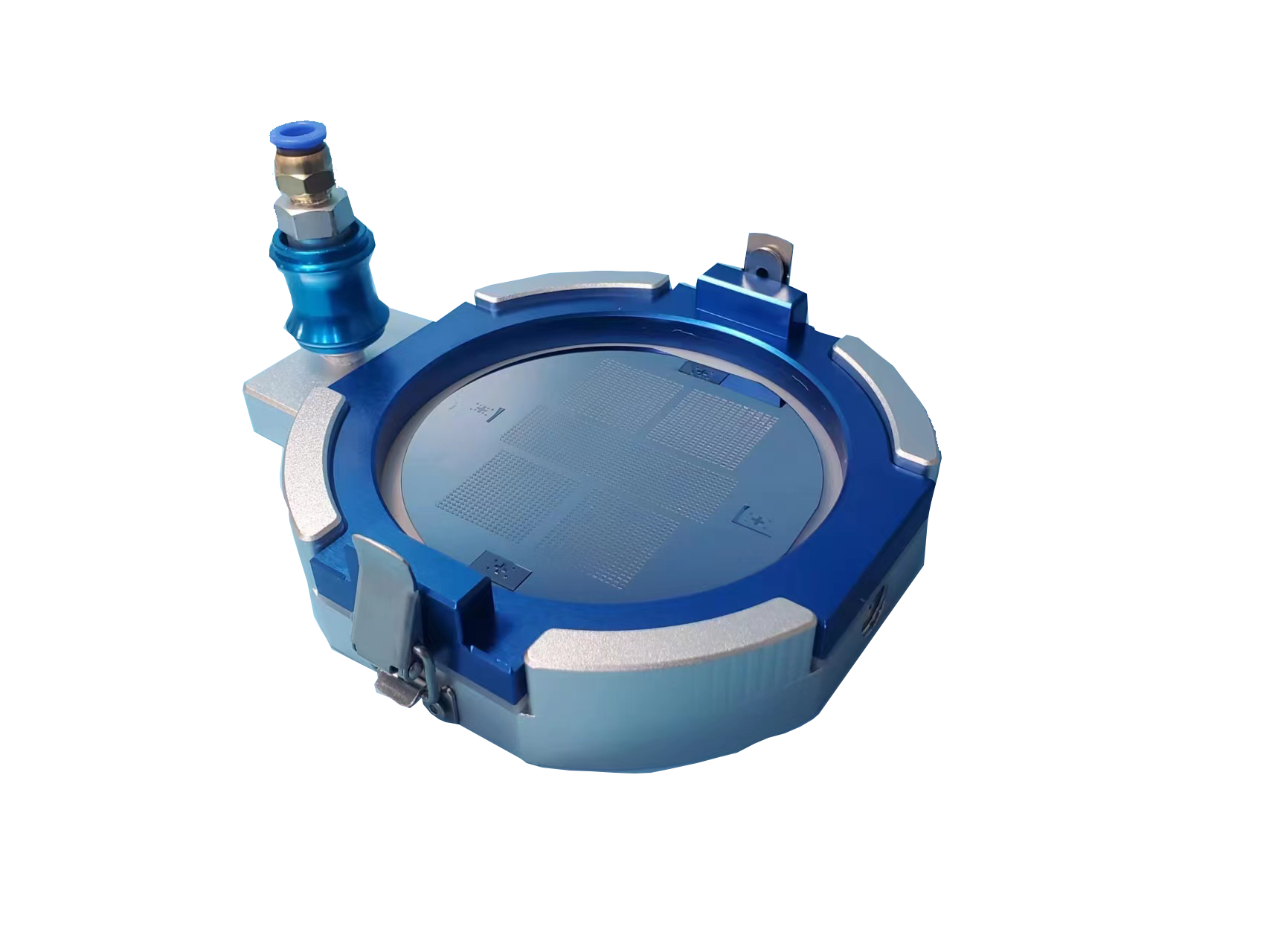
- Material: Aluminum Alloy
- Vacuum-absorbed silicon wafer
- Specifications: Suitable for casting on 4-inch and below SU8 molds or pure silicon molds
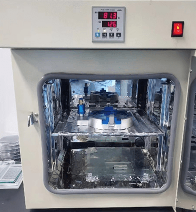
2.4 Oven
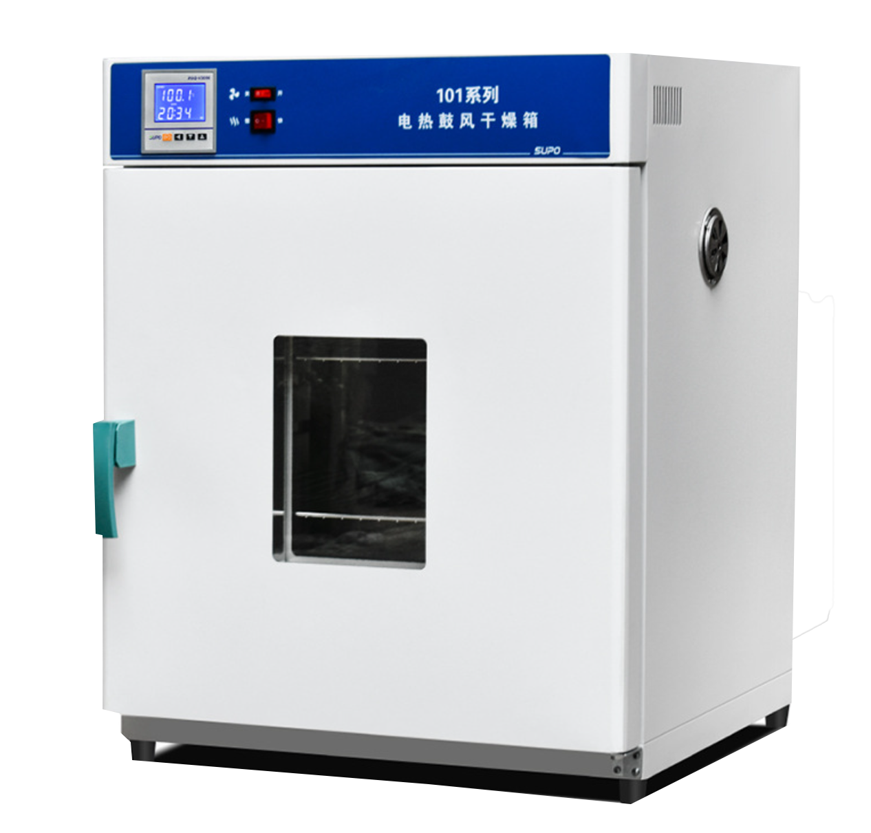
- Temperature Range: 10℃~300℃
- Temperature Resolution: 0.1℃
- Temperature Fluctuation: ±0.2℃
- Inner Material: Stainless Steel
- Inner Dimensions: 35x35x35cm (Length x Depth x Height)
- Outer Dimensions: 46x56x64cm (Length x Depth x Height)
- Power Supply: 220V
- Power: 0.8KW
2.5 Introduction to PDMS Chip Puncher
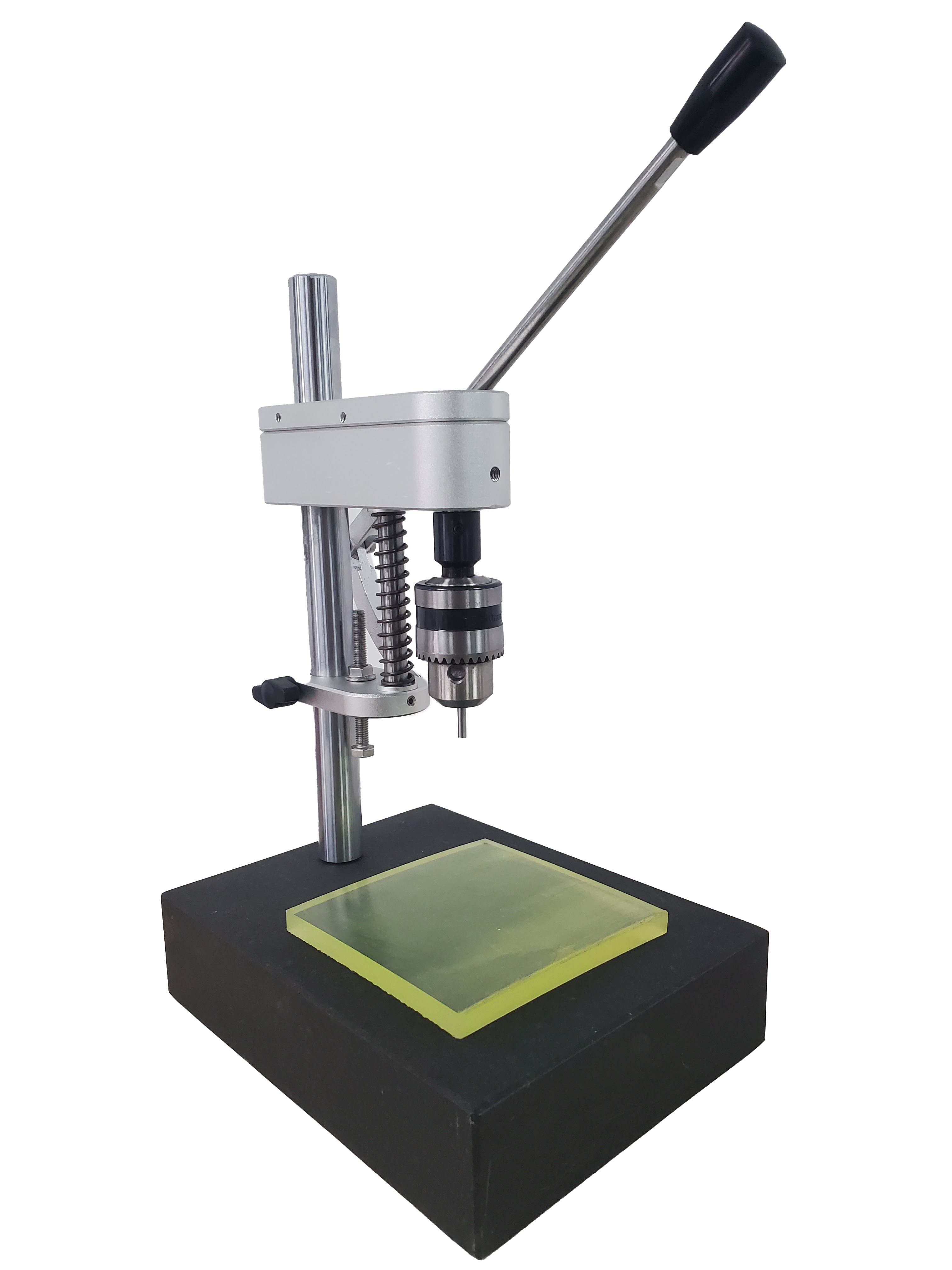
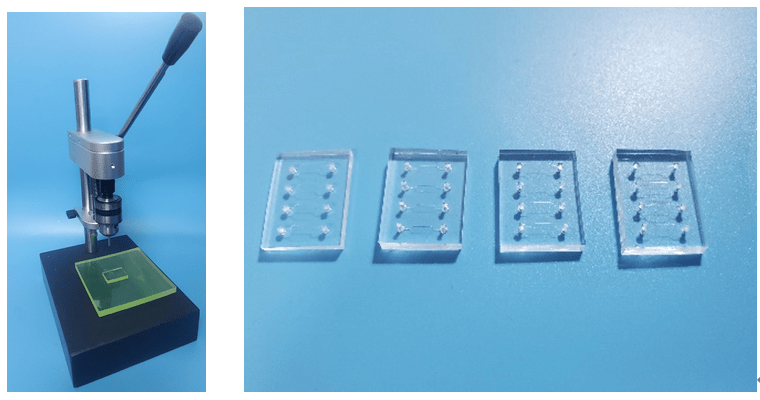
The PDMS chip puncher, inspired by the mechanical principles of a drill press, has undergone optimizations in its core structure, resulting in improved stability during operation. It is suitable for creating inlet holes in various soft microfluidic chips, such as PDMS chips and silicone chips. The desired hole depth can be adjusted through a positioning bolt (range: 0-20.0mm), and different inner diameter needle tubes (diameter range: 0.41-9.0mm) can be replaced to control the size of the inlet holes.
Needle Specifications
| Needle Specifications | Inner Diameter | Outer Diameter | Needle Specifications | Inner Diameter | Outer Diameter |
| 8G | 3.5mm | 4 mm | 16G | 1.2 mm | 1.6 mm |
| 10G | 3 mm | 3.5 mm | 17G | 1 mm | 1.5 mm |
| 11G | 2.5 mm | 3 mm | 18G | 0.85 mm | 1.3 mm |
| 12G | 2.3 mm | 2.8 mm | 19G | 0.7 mm | 1 mm |
| 13G | 2 mm | 2.4 mm | 20G | 0.6 mm | 0.9 mm |
| 14G | 1.6 mm | 2.1 mm | 21G | 0.51 mm | 0.8 mm |
| 15G | 1.4 mm | 1.8 mm | 22G | 0.41 mm | 0.7 mm |
2.6 PDMS Chip Cutter
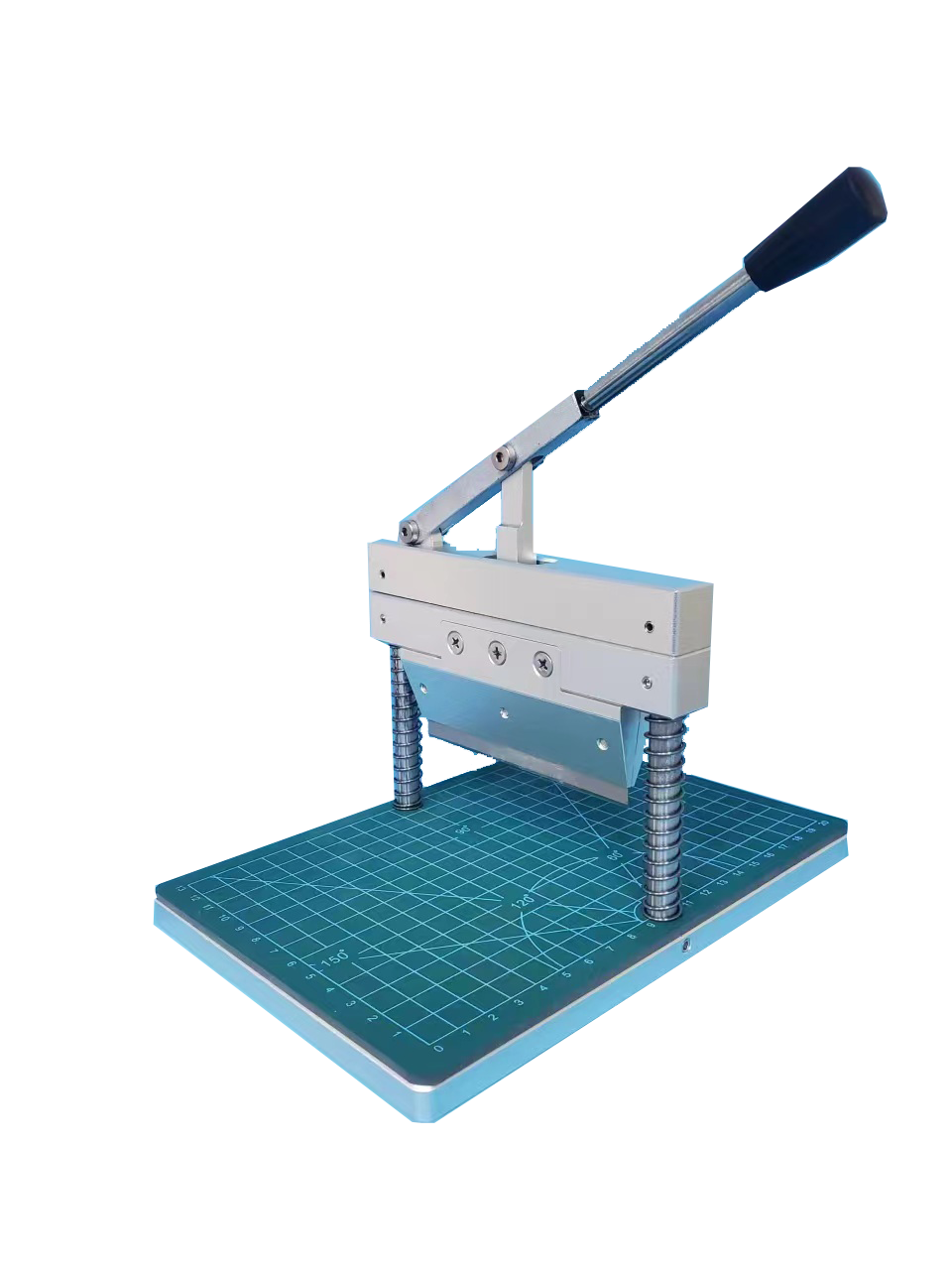
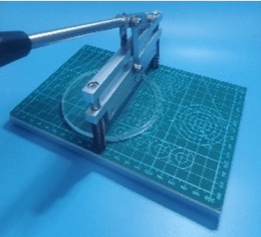
The PDMS chip cutter, inspired by the principles of a manual paper cutter, is designed for cutting PDMS (Polydimethylsiloxane) chips. This cutter ensures an efficient, precise cutting process, resulting in vertical and smooth edges, guaranteeing the quality and consistency of each cut chip. The blade specifications used are 100x18x0.35mm (length x width x thickness).
2.7 PDMS Chip Alignment Platform
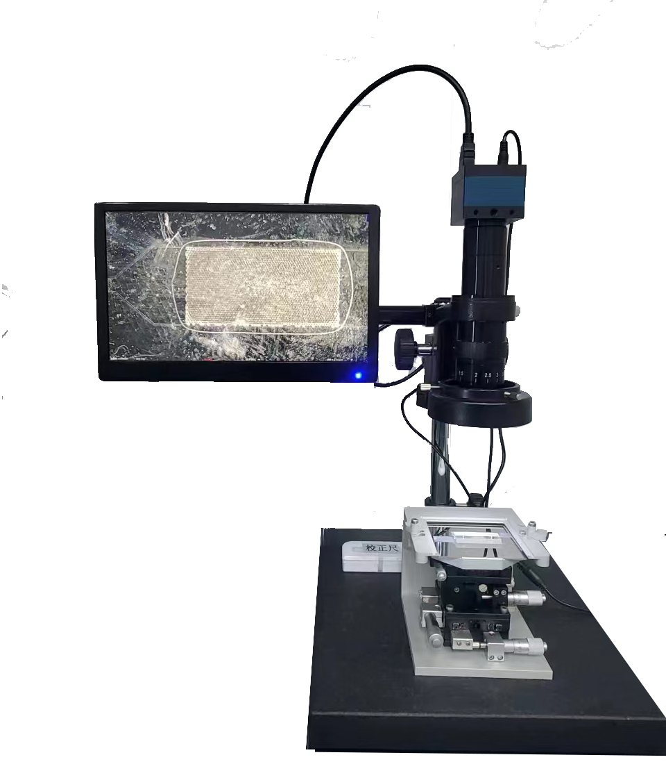
The PDMS chip alignment platform incorporates a mechanical displacement platform, integrating XYZ three-axis displacement and rotation functions. Combined with highly precise microscopy and advanced CCD imaging technology, it achieves precise control and visualization during the alignment process. The platform offers outstanding alignment accuracy and stability, suitable for bonding PDMS/PDMS, PDMS/glass, and PDMS/silicon chips with structures on both the upper and lower layers.
Main Technical Parameters:
Device Model: DZ-100
Suitable Samples: PDMS/PDMS, PDMS/glass, PDMS/silicon wafer
Alignment Accuracy: ±2um
Microscope Parameters:
Total Magnification: 20 ~ 200X continuous zoom
Objective Magnification: 0.7 ~ 4.5X continuous zoom
Eyepiece Magnification: 0.5X
Lifting Range: 270mm
Center Range: 150mm
Focusing Range: 65mm
Display Screen: 13.3-inch HD display
Camera Parameters:
Output Resolution: HDMI 1920x1080P
Chip Size: 1/2.8”
Supported Functions: Real-time display, capture, recording, measurement, etc.
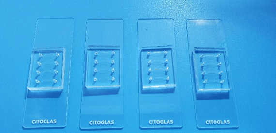
2.8 PDMS chip bonding
Plasma bonding machine for forming microchannels by tightly bonding polydimethylsiloxane (PDMS) to itself or to other materials (e.g. glass, silicon wafers).
PDMS chip bonding works like this:
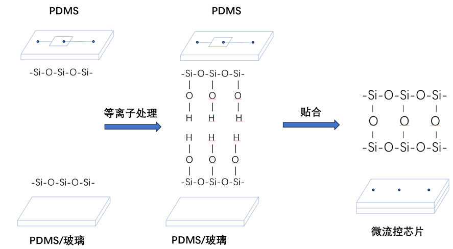
Under vacuum, air or oxygen is excited and ionized by a high-frequency power generator to form a plasma, which removes organic matter from the surface of the PDMS, exposing it to an atmosphere of highly reactive oxygen radicals and energetic oxygen ions, with which the hydrocarbons on the surface of the PDMS react to form silanol (SiOH) groups, which increase the hydrophilicity and wettability of the PDMS surface.
The plasma-activated PDMS was contacted with another PDMS or glass surface, and at the interface, the silanol groups formed stable and irreversible Si-O-Si covalent bonds with silanol groups or silica oxides on the other surface, forming a sealed and durable interface to complete the bonding of PDMS.
The principle of PDMS bonding
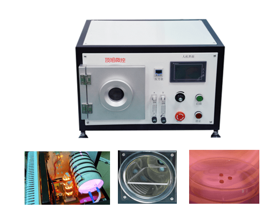
- Chamber Material: Quartz
- Power Supply: AC220V
- Operating Current: The overall operating current is not greater than 1.2A (excluding the vacuum pump).
- RF Power: Adjustable from 0 to 200W
- RF Frequency: 20.0MHz (offset less than 0.2KHz)
- Characteristic Impedance: 50 ohms, automatically matched
- Vacuum Level: 10Pa-30Pa
- Gas Channels: Dual gas input
- Gas Flow: Adjustable from 10 to 160ml/min
- Process Control: PLC human-machine interface with automatic and manual modes
- Cleaning Time: Adjustable from 1 to 6000 seconds
- Power Adjustability: 10% - 100%
- Inner Chamber Dimensions: Diameter 150mm × 270mm
- Overall Dimensions: 600mm × 500mm × 480mm
- Weight: 45Kg
- Vacuum Pump: Pumping speed of 4L/S
- Vacuum Chamber Temperature: Less than 30°C
- Cooling Method: Forced air cooling
3. PDMS Chip Preparation Process
The process for preparing a PDMS chip is as follows:
一、PDMSI. PDMS Pre-treatment
1) Use a disposable paper cup to weigh PDMS adhesive. Mix A and B adhesives at a mass ratio of 10:1, stirring the mixture with a stirring rod (or chopstick).
2) Degassing (Vacuum Deaeration)
Place the mixed PDMS adhesive in a vacuum deaerator, apply vacuum pressure to remove air bubbles from the mixture, and set aside for later use.
2 PDMS Pouring
1)Place the mold for chip preparation in the pouring tray.
2)Slowly pour the degassed PDMS into the tray, determining the thickness based on requirements, and let it stand for 10 minutes.
3 PDMS curing
Place the pouring tray in the oven for thermal drying, typically at a temperature of 70°C to 80°C for half an hour. Remove the PDMS after it has solidified.
4 Separation of PDMS
Open the latches on both sides of the PDMS pouring device, remove the upper part of the pouring device, and carefully take out the cured PDMS and mold together. Then, gently separate the PDMS from the mold.
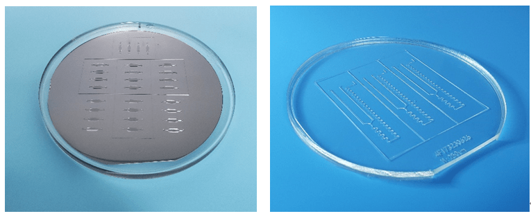
FIG1 SU8 mold+PDMS fig2 The separated PDMS
5 Cutting and Hole Preparation
1) Use the PDMS Chip Cutter to cut the PDMS chip according to the requirements, preparing the chip to the desired size.
2) Use the PDMS Chip Puncher to create the required holes on the chip for fluid inlet and outlet.
6 PDMS Chip Bonding
1) Use tape to clean the surface dust of the prepared PDMS chip.
2) Clean the glass substrate to ensure a clean and dust-free surface.
3) Place the processed PDMS chip and glass on a tray, then place it in a plasma chamber for surface treatment. If alignment of upper and lower layers is required for the PDMS chip, pre-align it using the alignment platform (but do not bond). Then, remove the completed PDMS chip along with the tray from the alignment platform and place it in the plasma chamber for surface treatment.
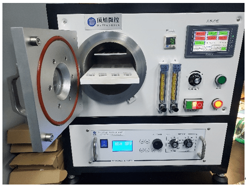
4) Affix the processed PDMS chip to glass quickly and place it in an oven at 85℃ for 30 minutes. If alignment of upper and lower layers is required, after plasma treatment, place the tray along with the aligned platform for alignment. After alignment, operate the Z-axis to raise the upper tray, allowing the PDMS layers to bond. Remove the assembly, place it in the oven at 85℃ for 30 minutes, and then remove the tray to complete the bonding process.
4 Consumables
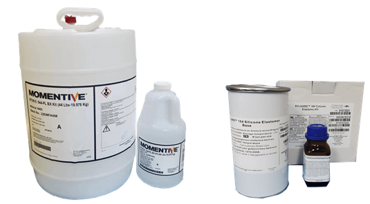
4.1 PDMS Adhesive
PDMS (Polydimethylsiloxane) is a widely used organosilicon-based polymer in the preparation of microfluidic chips. PDMS material is favored for its outstanding transparency, flexibility, and biocompatibility, making it an ideal choice for microfluidic chips. Key features of PDMS include:
> Optical Transparency: PDMS has excellent optical transparency, facilitating real-time imaging and microscopic observation, especially in applications such as microfluidic cell culture chambers.
> Low Cost and Easy to Manufacture: PDMS material is cost-effective and can be prepared through molding, and bonding can be achieved with simple plasma treatment.
> High Resolution and Fine Features: PDMS chips are typically made by pouring a liquid prepolymer onto a master mold. After curing, PDMS can precisely replicate the mold's structure, achieving micrometer-level accuracy.
> Biologically Inert: PDMS is a biologically inert material, maintaining neutrality in biological applications, making it a suitable choice for cell culture substrates.
> Permeability: PDMS is a permeable material, exhibiting good diffusion properties for oxygen and carbon dioxide, making it suitable for long-term cell culture. However, this may also lead to nonspecific adsorption of hydrophobic small molecules into microfluidic channels.
In microfluidic chip preparation, two main types of PDMS are commonly used: Momentive RTV-615 and Sylgard 184. While their compositions are proprietary, their performance is comparable. Therefore, the choice of suitable PDMS material depends on specific application requirements.
4.2 PDMS chip Mold
In the preparation of PDMS chips using the molding method, the selection of suitable molds is crucial for fabricating microstructured chips. Commonly used molds in the process of preparing PDMS chips include SU-8 molds, pure silicon molds, and acrylic molds. These molds play a critical role in microstructure fabrication, and their choice and design have a significant impact on the performance and application of the final chip.
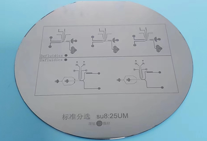
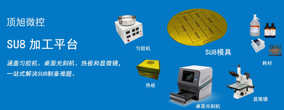
4.2.1 SU8 mold
SU-8 is a high-resolution negative photoresist with excellent mechanical, dielectric, chemical resistance, and thermal properties, along with outstanding biocompatibility. Molds prepared with SU-8 possess the following advantages:
1 High resolution and precision: SU-8 is a high-resolution photoresist, allowing the fabrication of complex and intricate microchannel geometries through photolithography. This results in well-defined microfluidic structures.
2 Tough and durable: SU-8 molds exhibit toughness and durability, enduring repeated use, cleaning, and handling without significant degradation. They are suitable for multiple PDMS chip castings.
SU-8 molds, utilizing photolithography processes, can manufacture line widths greater than 2 micrometers on SU-8 templates and achieve aspect ratios in structures ranging from 1:1 to 2:1. Additionally, with the aid of multilayer photolithography techniques, it is possible to create microchannel structures with different heights on SU-8 molds.
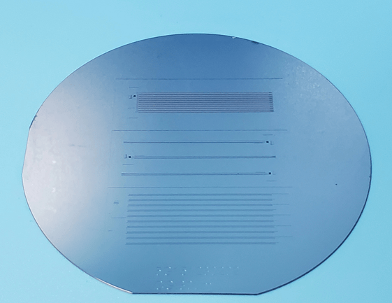
4.2.2 Silicon mold
Silicon molds are an ideal choice for preparing microchannels with high aspect ratios. Using silicon's dry etching technology, it is easy to achieve microchannel structures with a maximum aspect ratio of up to 25:1, and line widths can be controlled at 2 micrometers or more, with precision errors within the range of ±1 micrometer.
However, silicon surfaces typically exhibit strong hydrophilicity, which may lead to PDMS chips adhering to the silicon surface during demolding, posing a significant challenge in the manufacturing process. To address this issue, it is often necessary to perform hydrophobic modification on the silicon surface, making it hydrophobic to ensure easy detachment of PDMS chips from the silicon mold, without interference from hydrophilicity (specific hydrophobic solutions can be consulted with sales).
4.2.3 PMMA Mold
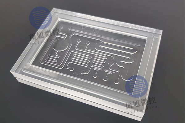
PMMA molds are known for their simplicity and cost-effectiveness in preparing PDMS chips. They can be precisely manufactured using CNC milling machines, and their surface exhibits some hydrophobicity, aiding in the easy demolding of PDMS material. These molds are suitable for fabricating microchannel structures with a width greater than 0.1 millimeters and an error control within around ±20 micrometers. PMMA molds are an ideal choice for applications with moderate precision requirements, offering cost-effectiveness and efficient preparation.
4.2.4 Resin Mold
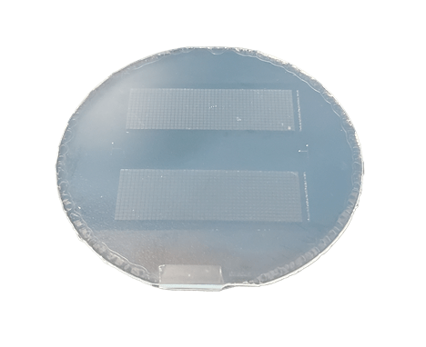
Resin molds are typically prepared by first creating PDMS chips using SU8 molds/pure silicon molds and then replicating them through PDMS molding. They offer several significant advantages:
> Epoxy resin molds can accurately replicate the microstructures of PDMS chips in a highly precise manner, maintaining the accuracy and clarity of fine features.
> Epoxy Resin molds are easy to demold, requiring no complex processing steps. They possess a reusable characteristic, greatly improving preparation efficiency and reducing costs. This feature is particularly beneficial for batch production and multiple experiments.
> The application of epoxy resin molds significantly reduces the frequency of using SU8 molds/pure silicon molds, effectively extending their lifespan. Compared to SU-8 or pure silicon molds, which are not only expensive to manufacture but also irreparable once damaged, resin molds can be reused multiple times. In the event of damage, they can be replicated again through PDMS chips. This process is simple and cost-effective, especially for large-scale production and repeated replication of high-precision microstructures in PDMS chip fabrication.Epoxy Resin molds, with their outstanding cost-effectiveness and reliability, demonstrate a clear competitive advantage.
Ordering Methods


Site Search
Recommendations
© 2025. All Rights Reserved. 苏ICP备2022036544号-1


