SU8The mold processing platform is designed to provide an efficient and comprehensive solution for SU8 mold processing, which integrates the core equipments such as desktop lithography, homogenizer and hot plate. Desktop lithography, with compact size and LED light source, has an exposure resolution of up to 2um and an exposure uniformity of more than 90%, which can realize the fine preparation of micro and nanostructures; Translated with DeepL.com (free version)
The leveling machine, with a speed stability of ±0.5% and a rotation speed of 10,000 rpm, ensures that the photoresist is uniformly coated and improves consistency; the hot plate, with a temperature stability of ±1%, provides SU8 molds with adequate baking, thus enhancing the durability and mechanical properties of the SU8 mold structure.
Compared to traditional processing platforms with bulky equipment and stringent environmental requirements, the SU8 mold processing platform is highly adaptable, with a small footprint for lithography, and can be easily deployed in ordinary laboratories.
SU8 mold processing platform, which is conducive to the rapid realization of chip preparation by customers and provides a convenient way for the promotion and application of microfluidic technology.
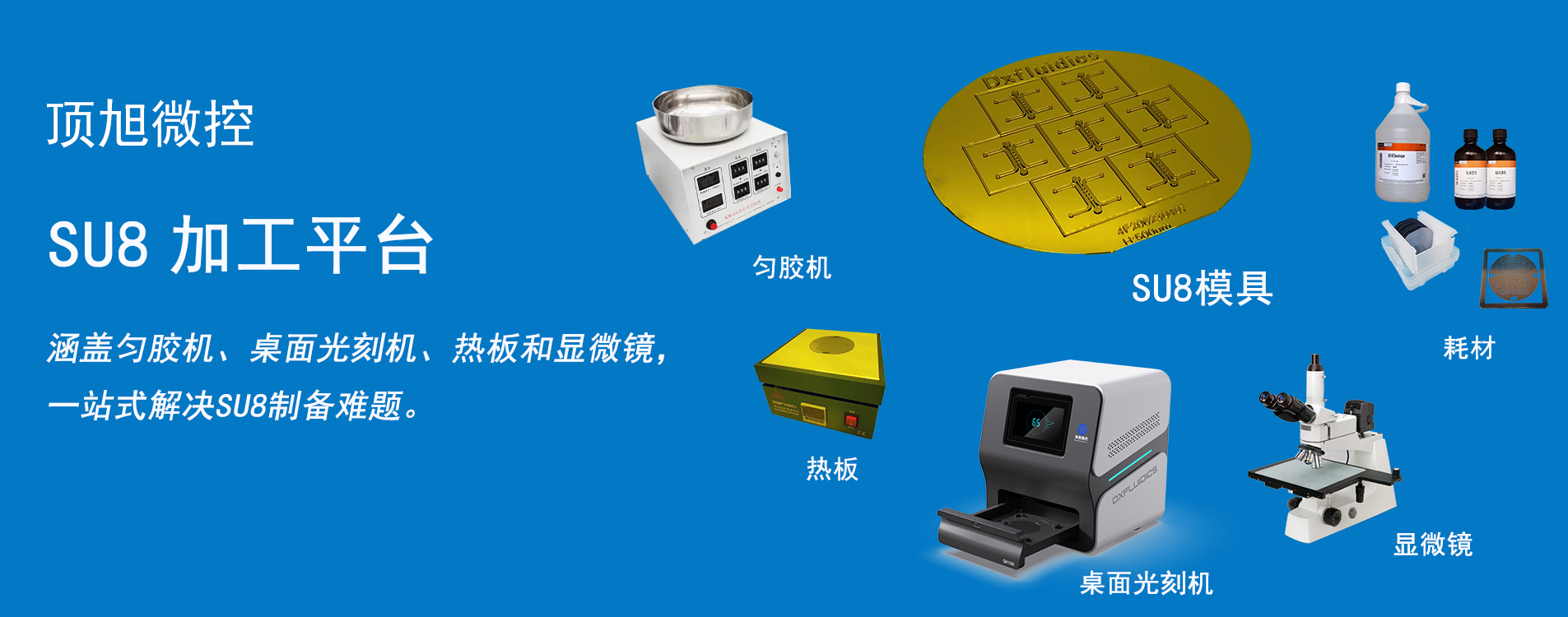
1 SU-8 Mold Processing Equipment
1.1 Desktop Photolithography Machine
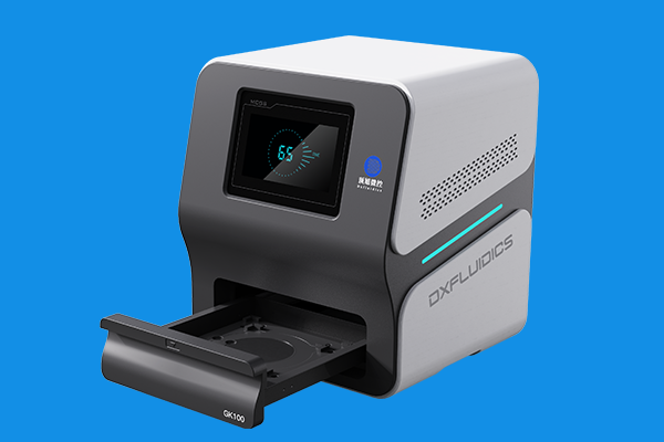
- Exposure Light Source: UV LED
- Wavelength of Light Source: 365nm
- Exposure Area: 4 inches, 6 inches optional
- Exposure Method: Single-side contact timed exposure
- Exposure Resolution: 2um
- Exposure Intensity: Adjustable from 20 to 200mW/cm22可调;
- Exposure Uniformity: ≤5%
- Light Source Parallelism: ≤2°
- Light Source Lifespan: ≥20,000 hours
- Power Supply Input: AC 220V ±10V, 50Hz
- Power Consumption: 250W
- Weight: 25kg
- Dimensions: 382 (Length) * 371 (Width) * 435 (Height)
- Operating Environment: Temperature 0℃-40℃, Relative Humidity <80%
1.2 Spin Coater
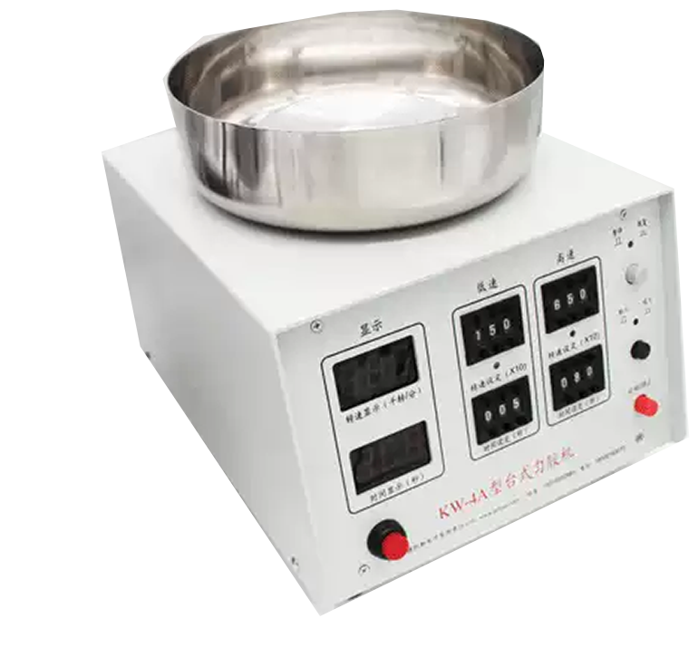
- Speed Range and Time:
I)Speed I: 50~10000 rpm, Time 0999s
II)Speed I: 50~10000 rpm, Time 0999s
- Applicable: Diameter 5~100mm silicon wafers and other material spin coating
- Speed Stability: ±1%
- Coating Uniformity: ±2%
- Electrode Power: 40W, Single Phase 110~240V
- Vacuum Pumping Rate: 60L/min
1.3 Hotplate
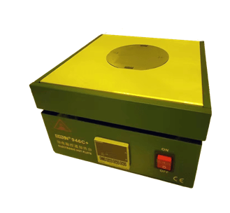
- Temperature: 0~300℃
- Temperature Stability: ±1℃
- Power: 850W
- Plate Size: 200x200mm
1.4 Digital Thickness Gauge (Micrometer)
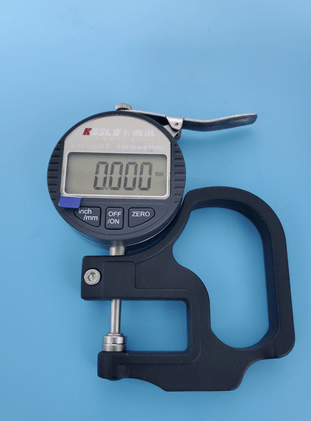
- Digital Thickness Gauge for Coating Thickness Measurement:
- Measurement Range: 0~10mm
- Accuracy: 0.001mm
- Tolerance: ≤±0.005mm
1.5 Microscope
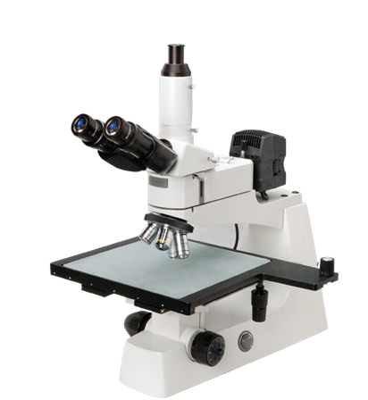
- Observation Head: Articulating trinocular observation head, inclined at 30°, interpupillary distance 48-75mm.
- Eyepiece: Super wide field eyepiece 10X/22.
- Infinity Plan Achromatic Objective: 4X/0.1, 10X/0.25, 20X/0.4, 40X/0.65.
- Converter: Quadruple converter.
- Stage: Stage area 300×268mm, movable range 250×250mm.
- Focusing: Coaxial coarse and fine focusing mechanism, 24mm travel.
- Illumination System: 6V20W halogen lamp, adjustable brightness.
- Filters: Blue, yellow, green, frosted glass.
2. SU-8 Mold Preparation Process:
2.1 Substrate Preparation: Retrieve clean silicon wafers from the chemical storage area, ensuring the surface is free from dust.
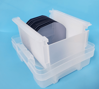
2.2 Spin Coating:
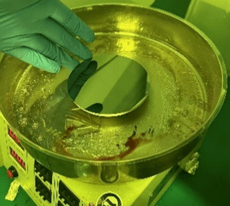
1)Turn on the spin coater, place the silicon wafer on the spin coater chuck, and activate the vacuum switch to secure the wafer in place.
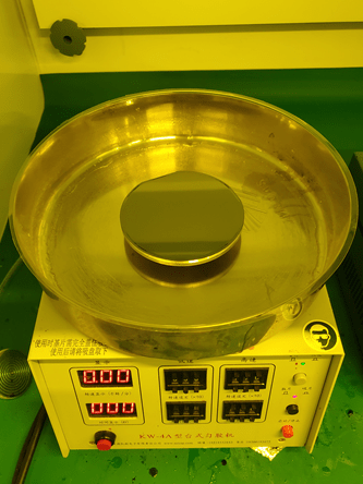
2)Dispense SU-8 photoresist onto the center of the wafer. Set the spin coater speed and time based on the desired photoresist thickness and fabrication requirements. (Example: Target thickness of 50 μm, SU8-2075, 1st step: 500 rpm for 8 s, 2nd step: 1800 rpm for 30 s)
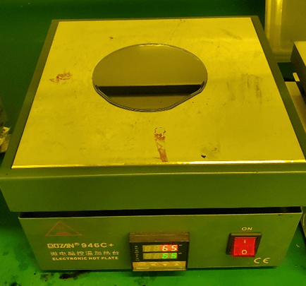
2.3 Pre-bake: Place the silicon wafer coated with SU-8 photoresist on a hotplate for pre-baking. This step helps remove volatile organic solvents from the photoresist. Adjust the time and temperature based on the thickness of the photoresist. (Example: Target resist thickness 50um, set temperature to 65℃, bake for 15 minutes, then increase the temperature to 95℃ and bake for an additional 15 minutes.)
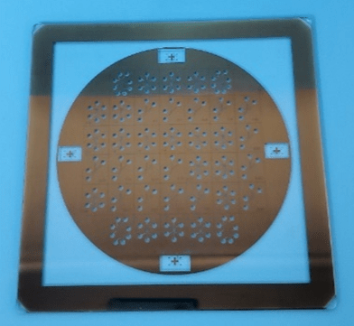
2.4 Exposure:Place the pre-baked silicon wafer on the tray of the desktop photolithography machine. Use the appropriate mask (photomask) and place it over the silicon wafer for exposure. Adjust the exposure time and intensity based on the type and thickness of the SU-8 photoresist. (Example: Target resist thickness 50um, set exposure energy to 25mW/cm2, exposure time 12 seconds.)
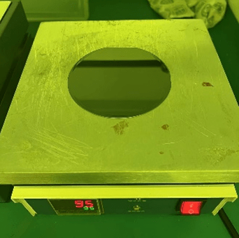
2.5 Post-bake: Place the silicon wafer, after exposure, on a hotplate for post-exposure baking to ensure the completion of the crosslinking reaction of the photoresist. (Example: Target resist thickness 50um, set temperature to 65℃, bake for 7 minutes, then increase the temperature to 95℃ and bake for an additional 3 minutes.)
2.6 Developing: Put the silicon wafer into the developer to dissolve the photoresist in the unexposed part and form the pattern of the mold. (Developing time is adjusted according to the thickness of the photoresist and the concentration of the developer, and the developing time here is 20min.)
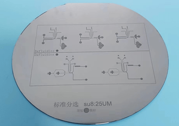
2.7 Cleaning: Clean the silicon wafer after development using isopropanol solvent to remove excess photoresist.
2.8 Inspection: Use a microscope to inspect the prepared SU-8 mold. Test and observe the dimensions of the microstructures, ensuring the clarity and quality of the pattern.
34 Consumables
3.1 Silicon
The silicon wafer does not have specific requirements and only requires single-side polishing. During the preparation of the SU-8 mold, the silicon wafer is polished, and the photoresist is spin-coated onto it.
3.2 Photomask
A photomask (also known as a mask reticle) is a master plate used in the SU-8 mold preparation photolithography process. It consists of an opaque light-blocking film forming microstructure patterns on a transparent substrate. During the exposure process, these microstructure patterns are transferred to the SU-8 photoresist coating, enabling precise replication of microstructures. Photomasks are generally categorized into film photomasks and glass photomasks.
Film mask plates are suitable for the preparation of structures with large line widths, usually above 20 microns. These masks are simple to prepare and are suitable for relatively wide and rough patterns.
However, due to its limited resolution, it is not able to meet the demand for the preparation of detailed microstructures. Therefore, for the need to prepare simple structures with line widths greater than 20 micrometers, a film mask plate is a suitable choice.
Glass mask plates are suitable for the preparation of fine structures with line widths of less than 20 micrometers, as well as for cases where multiple layers need to be aligned. Glass mask plates are more complex to prepare, but due to their high resolution, more detailed and precise microstructures can be realized.
Especially in the case of complex multilayer structures that need to be prepared and require high alignment accuracy, glass mask plates have obvious advantages.
The choice of mask plate type should be weighed against the characteristics of the pattern to be prepared, the width of the lines, and the requirements for precision and complexity of the preparation. Film mask plates are suitable for relatively simple structures, while glass mask plates are better suited for the preparation of more detailed and complex microstructures.
Taking into account the preparation goals and technical requirements, selecting the appropriate mask plate type will help ensure the success and efficiency of the preparation process.
3.3 Photoresist
SU-8 is a commonly used negative photoresist composed of epoxy resin and photosensitive agents. It has several advantages that make it an ideal choice for preparing microstructures and devices:
- High resolution: SU-8 photoresist has excellent resolution, allowing the fabrication of intricate microstructures suitable for small-sized lines and fine patterns.
- Strong adhesion: SU-8 photoresist exhibits good adhesion to many substrate surfaces, enabling the preparation of microstructures on different materials.
- Adjustable thickness: SU-8 photoresist thickness can be controlled through multiple coating and lithography processes, suitable for preparing microstructures of varying thicknesses.
- Chemical stability: SU-8 photoresist has high chemical stability, tolerating many solvents and chemicals, making it suitable for various application environments.
- Thermal stability: SU-8 photoresist exhibits good stability at high temperatures, suitable for processes requiring high-temperature treatment.
- Multi-layer lithography: SU-8 photoresist can be used for multi-layer lithography, enabling the fabrication of more complex microstructures and devices.
Wide applications: SU-8 photoresist finds extensive applications in various fields, including microfluidic devices, biochips, MEMS, optical devices, and more.
Ordering Methods


© 2025. All Rights Reserved. 苏ICP备2022036544号-1


