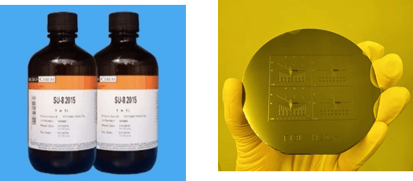
SU-8 photoresist
SU-8 photoresist is a high-resolution, high-precision, high-adhesion negative photoresist, which is widely used in the field of micro and nanofabrication. In microfluidic chips, SU-8 photoresist is widely used in the preparation of microfluidic chips, which can be used to prepare microstructures such as microfluidic channels, reaction chambers, valves and pumps.
Specifically, the application of SU-8 photoresist in microfluidic chips can be categorized into two aspects: the preparation of microstructures and the packaging of microfluidic chips.
1. Preparation of microstructures
SU-8 photoresist can be used to prepare SU8 molds for casting PDMS chips.SU-8 photoresist can be used to prepare microstructures such as microfluidic channels, reaction chambers, pumps, valves, etc. through the photolithography process.
Compared to other materials, SU-8 photoresists offer stronger adhesion and higher precision, allowing for the preparation of more complex and finer microstructures. In addition, SU-8 photoresists are highly resistant to chemicals and high temperatures, allowing them to withstand more demanding microfluidic conditions.
2. Packaging of microfluidic chips
During the preparation of microfluidic chips, microstructures need to be encapsulated to ensure the stability and reliability of microfluidic chips.
SU-8 photoresist can be used as one of the encapsulation materials for microfluidic chips, which can be used to prepare the upper and lower covers of microfluidic chips, as well as the connectors and seals of microfluidic chips.
In conclusion, the application of SU-8 photoresist in microfluidic chips is of great significance, which can realize the high-precision preparation and encapsulation of microfluidic chips, and provide a strong support for the research and application of microfluidic chips.
SU-8 photoresist model
Common models of SU-8 photoresist are listed below:
| SU-8 2000series | Single spin coating film thickness range |
| SU-8 2002 | 1~4um |
| SU-8 2005 | 3~8um |
| SU-8 2010 | 7~15um |
| SU-8 2025 | 15~40 |
| SU-8 2050 | 20~100um |
| SU-8 2075 | 50~200um |
| SU-8 2100 | 80~250um |
| SU-8 2150 | 130~400um |

developer
A developer is a chemical solution used in the photolithography process, primarily to remove portions of unexposed areas from the photoresist pattern to create the desired microstructure. The composition and formulation of a developer solution will vary depending on the type and use of the photoresist, and will generally contain the following key ingredients:
1. Alkaline solution: The developer solution usually contains an alkaline substance, such as sodium hydroxide, sodium bicarbonate, etc., which is used to remove unexposed photoresist areas. The concentration and type of alkaline solution needs to be adjusted to the specific photoresist type and thickness.
2. Promoter: Promoter can accelerate the development process, improve the efficiency and speed of development, usually used promoter ammonia, ethylenediamine and so on.
3. Inhibitors: Inhibitors are used to inhibit the etching rate of the developer in the exposed area of the photoresist, thus preventing excessive removal of the photoresist. The type and concentration of the inhibitor also needs to be adjusted according to the type and thickness of the photoresist.
4. Deionized water: Deionized water is a solvent in the developer, used to dilute the developer and rinse the chip after development, thus reducing the corrosion and pollution of the chip material.
In conclusion, the developer is an indispensable part of the photolithography process, and its composition and formulation need to be selected and adjusted according to the specific experimental needs and photoresist type to ensure the accuracy and stability of the photolithography effect and experimental results.
© 2025. All Rights Reserved. 苏ICP备2022036544号-1


