photolithography
Photolithography is the use of exposure and development techniques to etch the device structure on the photoresist layer, and then the graphics on the mask are converted to the substrate through the etching process. The main photolithography are: electron beam lithography, step lithography, contact lithography and many other photolithography techniques.

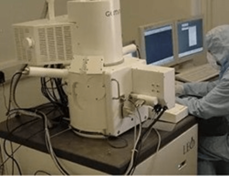
electron beam lithography (EBL)
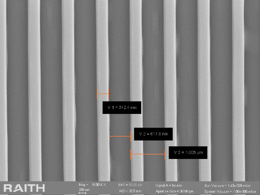
Minimum line width of 50nm (proven), suitable for processing on conductive substrates and small graphic areas.

Projection/step lithography
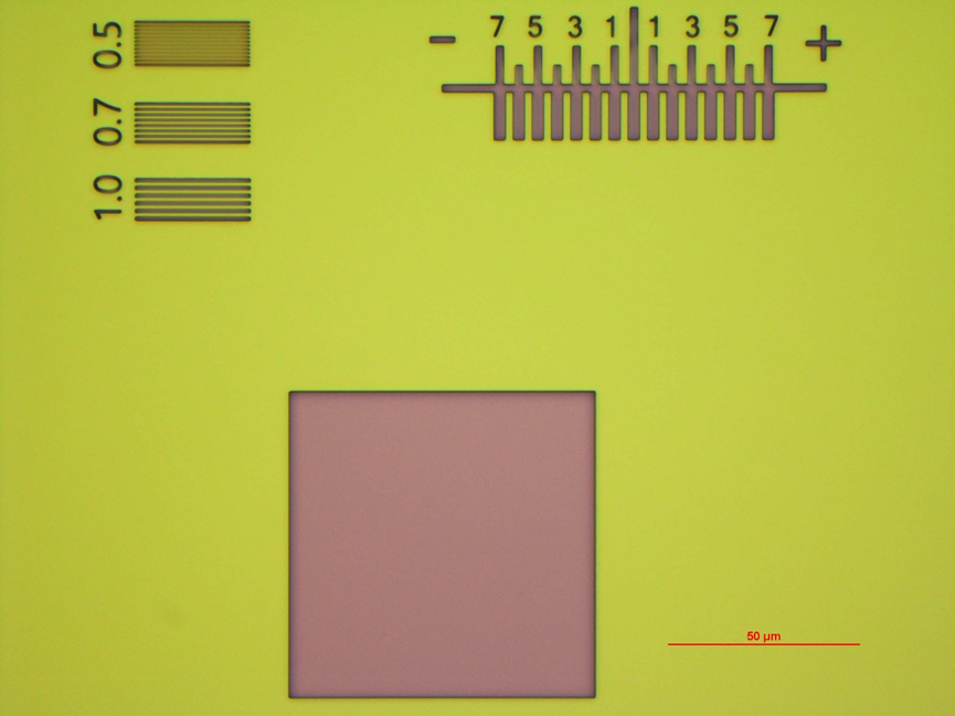
stepper i7/i10/i12, minimum linewidth 500nm, suitable for small lines plus demand workers.

Contact, proximity lithography
MA6/BA6 lithography, minimum line width 2um, suitable for positive and negative registration, high substrate inclusivity

Case Studies


Site Search
Recommendations
© 2025. All Rights Reserved. 苏ICP备2022036544号-1


