MEMS Fabrication
More than 10 years of experience in MEMS processing, providing full-process MEMS foundry such as coating, lithography, metal, etching, dicing, ion implantation, and electron beam lithography.
More than 10 years of experience in MEMS processing, providing full-process MEMS foundry such as coating, lithography, metal, etching, dicing, ion implantation, and electron beam lithography.
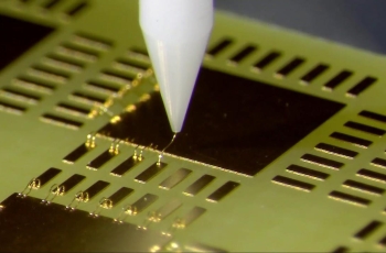
It refers to the process of processing the tested wafers according to the product model and functional requirements to get an independent chip, and the processes involved include: slicing (scribing), patching, leading and bonding.
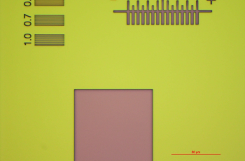
Photolithography is the use of exposure and development techniques to etch the device structure on the photoresist layer, and then the graphics on the mask are converted to the substrate through the etching process. The main photolithography are: electron beam lithography, step lithography, contact lithography and many other photolithography techniques.
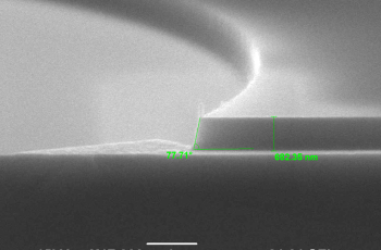
Etching technology is not only a fundamental manufacturing process for semiconductor devices and integrated circuits, but is also applied to thin-film circuits, printed circuits and other microfabrication.
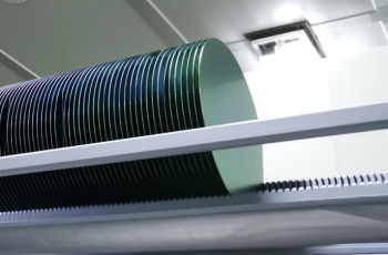
Coating is a technique in which a material (commonly known as a target or film) is deposited on the entire surface of a substrate under vacuum conditions using physical bombardment or chemical reaction.