SU-8 is a high-resolution negative photoresist known for its outstanding mechanical, dielectric, chemical resistance, and thermal properties, as well as excellent biocompatibility. In the field of microfluidics, it is commonly used to fabricate molds for preparing PDMS microfluidic chips.
Molds prepared with SU-8 offer the following advantages:
1 High resolution and precision: SU-8 is a high-resolution photoresist, allowing the fabrication of complex and intricate microchannel geometries through photolithography. This results in well-defined microfluidic structures.
2 Tough and durable: SU-8 molds exhibit toughness and durability, enduring repeated use, cleaning, and handling without significant degradation. They are suitable for multiple PDMS chip castings.
3 SU8 molds, created using photolithography, can produce line widths greater than 2 micrometers on PDMS chip molds prepared with SU-8 photoresist. Achieving aspect ratios in the range of 1:1 to 2:1 is possible. Additionally, employing multilayer photolithography techniques allows the creation of microchannel structures with different heights on SU-8 molds.
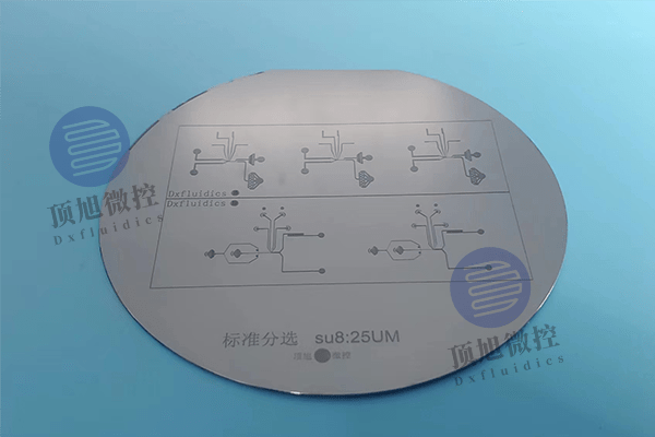
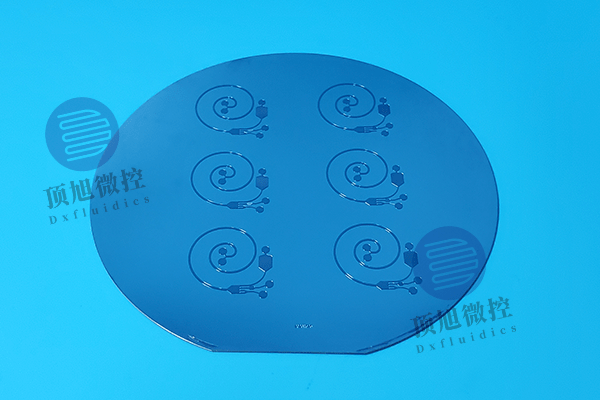
Equipment for Fabricating SU8 Molds

For more details, please click onSU-8 Processing Equipmentto learn more
SU-8 Mold Preparation Process:
I. Substrate Preparation
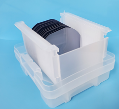
Retrieve a clean silicon wafer from the chemical storage area, ensuring the wafer's surface is dust-free.
II. Spin Coating
1)Turn on the spin coater, place the silicon wafer on the spin coater chuck, and activate the vacuum switch to secure the wafer in place.
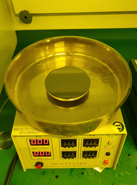
2)Dispense SU-8 photoresist onto the center of the wafer. Set the spin coater speed and time based on the desired photoresist thickness and fabrication requirements. (Example: Target thickness of 50 μm, SU8-2075, 1st step: 500 rpm for 8 s, 2nd step: 1800 rpm for 30 s)
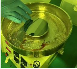
III. Soft Bake
Place the coated silicon wafer on a hotplate for a pre-bake to remove volatile organic solvents from the photoresist. Adjust time and temperature according to the photoresist thickness. (Example: Target thickness of 50 μm, set temperature to 65°C, bake for 15 min, then raise temperature to 95°C, and bake for an additional 15 min)
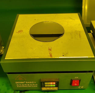
IV. Exposure
1)Place the pre-baked silicon wafer on the tabletop mask aligner tray.
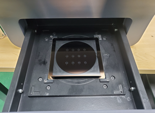
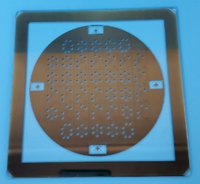
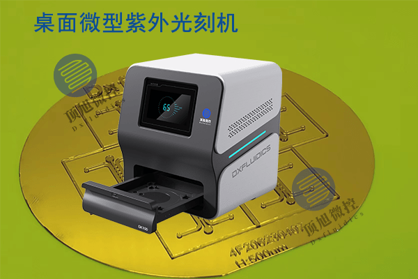
2)Expose the wafer using an appropriate mask. Adjust exposure time and intensity based on the type and thickness of SU-8 photoresist. (Example: Target thickness of 50 μm, set exposure energy to 25 mW/cm2, exposure time of 12 s)2,时间12s)
V. Post-Bake
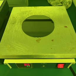
Place the exposed silicon wafer on a hotplate for post-exposure baking to ensure completion of the cross-linking reaction in the photoresist. (Example: Target thickness of 50 μm, set temperature to 65°C, bake for 7 min, then raise temperature to 95°C, and bake for an additional 3 min)
VI. Development
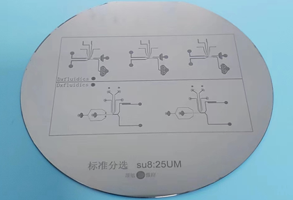
Immerse the wafer in a developer solution to dissolve the unexposed portion of the photoresist, forming the pattern of the mold. (Adjust development time based on photoresist thickness and developer concentration; example: development time of 20 min)
VII. Cleaning
Clean the developed wafer with isopropanol solvent to remove excess photoresist.
VIII. Inspection
Use a microscope to inspect the prepared SU-8 mold, checking the dimensions of the microstructures, and confirming the clarity and quality of the pattern.
Ordering Methods


Site Search
© 2026. All Rights Reserved. 苏ICP备2022036544号-1


.png&w=120&h=120&zc=1&q=100)


