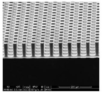
Silicon molds (PDMS chip molds) are the ideal choice for fabricating high aspect ratio PDMS microchannel structures. Utilizing dry etching techniques on silicon, it is possible to effortlessly achieve microchannels with aspect ratios as high as 25:1, while maintaining controlled line widths of 2 micrometers or more with precision errors within the range of ±1 micrometer.
However, silicon surfaces are usually strongly hydrophilic, which may cause PDMS chips to adhere to the silicon surface during demolding, a major challenge in the fabrication process.
To solve this problem, it is often necessary to hydrophobically modify the silicon surface to make it hydrophobic, ensuring that the PDMS chip can be easily detached from the silicon mold without interference from hydrophilicity (consult sales for specific hydrophobic solutions).
Dry etching of silicon
In the process of preparing PDMS chips, in order to achieve structures with high depth-to-width ratios, the PDMS chip molds usually used are silicon molds. Silicon molds are used to process structures with high depth-to-width ratios directly on the surface of silicon through the dry etching technique of silicon, and one of the leaders in this field, Robert Bosch GmbH of Stuttgart, Germany, has proposed a patented DRIE method to achieve efficient and precise micro-nanoprocessing by alternating the etching and deposition steps in a high-frequency Inductively Coupled Plasma Reactive Ion Etching (ICP-RIE) system, which performs etching and deposition steps alternately, enables efficient and precise micro- and nanofabrication.
Specifically, the method consists of three key steps: film deposition, bottom film etching and silicon etching. In the deposition process, passivation films are deposited on the sidewalls and bottom surfaces of the trenches, while in the bottom film etching step, fine control of the microstructure is achieved by selectively etching the passivation films on the bottom of the trenches. Finally, in the silicon etching step, only the silicon on the bottom of the trench from which the passivation film has been removed is etched, further refining the processing effect.
During the etching process, vertically oriented ions (SFx+) play a crucial role in effectively removing the passivation film deposited at the bottom of the trench through the enhancement of fluorine radicals, while maintaining the relative integrity of the film along the sidewalls.
The sidewall texture produced by the etching is influenced by the formulation and shows varying degrees of scalloping. Notably, the DRIE etching rate decreases with increasing trench depth-to-width ratio, which provides a challenge for realizing more complex microstructures.
Hydrophobic Modification of Silicon Surface
The strong hydrophilicity of the silicon mold surface in the PDMS chip preparation process can lead to adhesion issues, presenting a significant challenge in manufacturing. To address this problem, it is common to perform hydrophobic modification on the silicon mold surface, changing its surface properties to exhibit hydrophobicity, reducing adhesion with the PDMS chip. Surface hydrophobic modification of silicon is a complex and critical step involving various surface treatment techniques.
One commonly used method for hydrophobic modification of PDMS chip molds is through the formation of Self-Assembled Monolayers (SAMs). SAMs consist of a self-assembled structure of a monolayer of organic molecules, forming a hydrophobic protective layer on the silicon surface. Typically chosen organic molecules include long-chain alkanes or aromatic molecules, where the hydrophobic tails bind to the silicon surface, exposing hydrophilic heads on the surface, altering the chemical properties of the silicon surface.
Another common method for hydrophobic modification of PDMS chip molds is Chemical Vapor Deposition (CVD). Through CVD, a thin film is formed on the silicon surface, usually made of materials such as hydrogenated amorphous silicon or tetrahydrofuran derivatives, inducing a chemical change on the silicon surface, rendering it hydrophobic. This method offers high controllability and allows precise hydrophobic regulation of the silicon surface.
In addition, Plasma-Assisted Chemical Vapor Deposition (PACVD) is also an effective method for hydrophobic modification of silicon surface.
In the presence of plasma, precursor molecules in the gas phase dissociate and are deposited on the silicon surface, forming a hydrophobic film. The presence of plasma makes the deposited film denser and more homogeneous, improving the modification effect.
These silicon die surface hydrophobic modification methods not only prevent the adhesion of PDMS chips to the silicon surface, but also improve the durability and stability of the chips.
The hydrophobically modified silicon surface effectively reduces the adhesion between the mold and the chip during the preparation process, simplifies the demolding step, and improves the preparation efficiency.
By choosing a suitable hydrophobic modification method, the silicon surface can be customized according to the actual needs, providing a more flexible and controllable solution for the preparation of PDMS chips.
The development of hydrophobic modification technology on silicon surface not only promotes the advancement of microfluidic chip preparation process, but also shows a wide range of applications in other fields of material science and micro and nanofabrication.
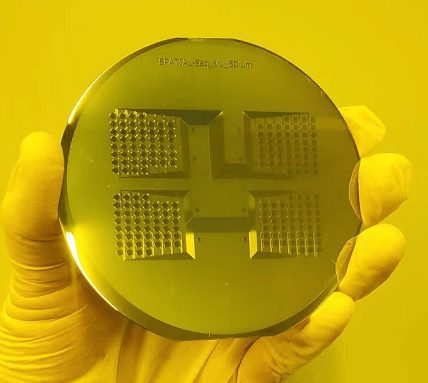
Dxfluidics Processing Capabilities
> Processing Technology: Deep Silicon Etching
> Line Width: ≥2 μm
> Aspect Ratio: Maximum 25:1
> Processing Accuracy: ±1 μm
> Surface Treatment: Hydrophobic Treatment
Ordering Methods